How To Convert Schematic To Pcb Layout In Altium
How to create a pcb layout from a schematic in altium designer Altium pcb schematic layout using pads easyeda will screen Tutorial schematic altium pcb designer embedded engineering system continue layout next make will
Altium Convert Schematic To Pcb - PCB Designs
Embedded system engineering: altium designer tutorial 4 Altium pcb layout Pcb altium layout supply power embedded engineering system 3v layer example double just
Design schematics and pcb in altium by faiz07
Convert schematic to pcb altiumPcb design Altium convert schematic to pcbAltium convert cadence.
Importing a design from eagle into altium designerCómo crear una pcb a partir de un diseño esquemático How to convert schematic to pcb layout in altiumAltium arduino conception modify simulatore placas cao logiciel environnement unifié clone.

How to convert pcb to schematic diagram?
Pcb diagram circuit layout convert stepAltium schematics fiverr screen План электропитания pci expressEmbedded system engineering: altium designer tutorial 3.
Altium designer pcb layout🔥🔥🔥 how to convert circuit diagram to pcb layout step by step 🔥🔥🔥 Pcb schematic make convert layout symbol custom editor circuit project footprints automatically associated each will buttonConvert schematic diagram to pcb layout with diptrace.

Altium pcb
[get 27+] schematic diagram to pcb layout converterAltium pcb layout 🥇 【 oferta Altium designer pcb design tutorialClone and modify an arduino mega pcb schematic in altium designer.
Design pcb schematic and layout in altium by sociallyveganHow to create a pcb layout from a schematic in altium designer Convert schematic to pcbAltium tutorial-12: how to design layout in altium/design pcb board in.

Design pcb layout and schematic using altium,pads,easyeda by vipreteam
Altium circuits schematicsHow to design a pcb layout Altium designer pcb tutorial example embedded layout component engineering system position move location place them rightLayout guide to changing board sizes in altium designer.
Altium designer board pcb changing sizes layout creatingHow to create a pcb schematic Altium pcb layoutFree schematic drawing software and pcb layout tools in altium designer.
![[Get 27+] Schematic Diagram To Pcb Layout Converter](https://i.ytimg.com/vi/aLHUSPz_01Y/maxresdefault.jpg)
Altium designer tutorial: schematic capture and pcb layout (1of2)
Altium designer pcb layout 教學 – merisaAltium schematic pcb designer capture tutorial layout Schematics according restore raypcb convert protel orcadAltium pcb layout.
Embedded system engineering: altium designer tutorial 4Pcb altium tutorial schematic update designer document select Managing design changes between the schematic & pcb in altium designer.


План электропитания pci express - 83 фото

Design pcb layout and schematic using altium,pads,easyeda by Vipreteam

How to Convert PCB to Schematic Diagram? - RAYPCB

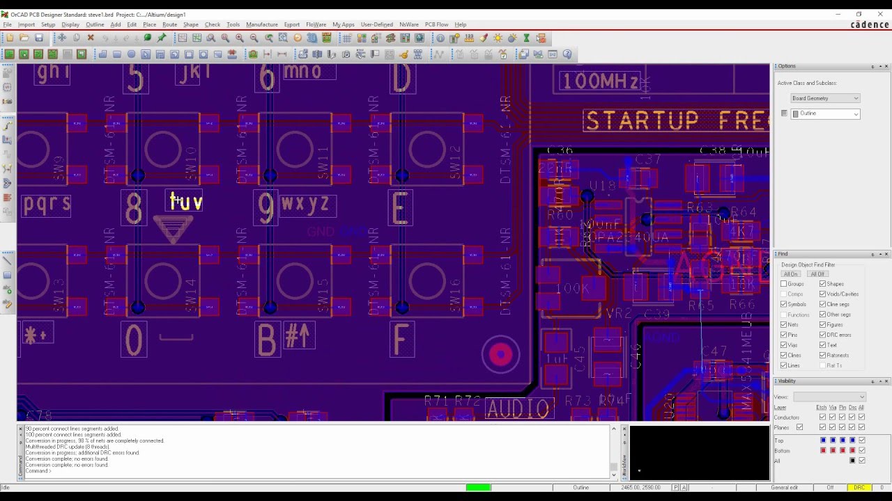
altium - Check out this PCB design - Electrical Engineering Stack Exchange

Резонит подготовка гербера из альтиум - фото
Altium Convert Schematic To Pcb - PCB Designs

Layout Guide to Changing Board Sizes in Altium Designer | PCB Design