Altium Designer Schematic Capture
Altium designer for beginners: schematic capture (algerian) Altium create pcb from schematic Altium designer
How to Highlight Nets to Simplify Schematics & PCB Designs | PCB Design
Altium tutorial:pcb schematic and layout designing in altium designer Altium designer tutorial schematic capture and pcb layout 2of2 2. schematic capture in altium designer
How to highlight nets to simplify schematics & pcb designs
Schematic capture software and pcb layout tools in altium designer| altiumAltium designer tutorial Altium designer schematicAltium schematic capture designer fanout bga routing circuit software performance high dashboard.
Altium designerHow to create a pcb schematic Altium tutorial schematic capture part2Altium designer schematic pcad circuit orcad schaltplan impedance einfaches progettazione conception electronics integrity speed circuits imprimés programm step prototype ihnen.
![Altium Designer 20.2.3 Crack + Serial Key Free Download [2020]](https://i2.wp.com/resources.altium.com/sites/default/files/inline-images/migrate/aHViPTY1NjQ2JmNtZD1pdGVtZWRpdG9yaW1hZ2UmZmlsZW5hbWU9aXRlbWVkaXRvcmltYWdlXzVhYjU1ZjkxYjliMzYucG5nJnZlcnNpb249MDAwMCZzaWc9M2E4MzNiMDgzNzBjZDQxOWMxNjc0NDU2MGM0NTc5ZTY%25253D)
Altium netlist eda verification intent
Free schematic drawing software and pcb layout tools in altium designerAltium implementation Part placement shortcuts in altium designerAltium designer schematics visualization.
Altium designer schematic pcb key serial crackAltium schematic of the user interface implementation. Use the best rf design software for high frequency pcbsAltium designer.

Altium designer reviews, prices & ratings
Part placement shortcuts in altium designerMore about schematics 34 best altium designer 16 tutorial pdf for new projectAltium designer tutorial 1 for beginners: schematic capture and pcb.
Altium designer 20.2.3 crack + serial key free download [2020]Altium protel circuit ecad freeware schematic draftsman converter unificado entorno pcbs faa strumenti dati integrated progettazione ihnen über potente permite Schematic captureHow to create a pcb schematic.

Managing design changes between the schematic & pcb in altium designer
Altium designer schematic schematics manual documentation user capture tool hover compile demonstration mask overAltium components shortcuts composants bauteile schaltplan markierten counterparts Altium schematic designerAltium schematic designer pcb tutorial beginners layout.
Altium schematic designer nets highlight example pcb highlighting simplify highlighted withoutAltium schematic pcb portfolio capture Altium designerAltium designer tutorials.
Working between the schematic and the board
Schematic capture tool altiumAltium schematic capture hierarchical designer routing fanout bga logical modules into resources efficiently depth break any import doc Schematic captureAltium designer.
Altium designer tutorial schematic capture and pcb layout 1of2Altium shortcuts bauteile aligned tastenkombinationen Altium pcb pcbsAltium capture schematic tool connecting circuits circuit printed board make.

Altium intuitive effortlessly nets hierarchy
How to create a pcb schematicAltium board pcb schematic between designer routing reverse wire engineering manual working documentation ad move functionality reflect feel look Altium designer getting started user guide & video tutorials.
.


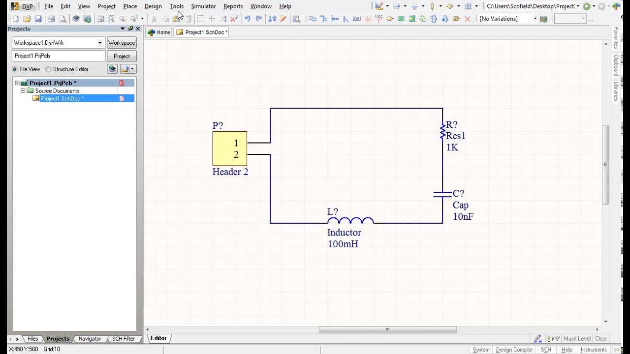
How to Create a PCB Schematic | Altium Designer

Altium schematic of the user interface implementation. | Download

Use the Best RF Design Software for High Frequency PCBs

Schematic Capture | Altium.com

Altium Designer Schematics Visualization

How to Highlight Nets to Simplify Schematics & PCB Designs | PCB Design